Solid-State Transformer Deployment Accelerates As China Achieves Breakthroughs in KV-Class SiC Power Devices
China’s Breakthroughs in kV-Class SiC Power Devices: Accelerating Solid-State Transformer Commercialization
Two major advancements in the field of wide-bandgap semiconductors have recently been announced in China: a 15 kV bidirectional-blocking SiC power device developed by Dr. Xing Huang’s team at Pinejade, and a 10 kV SiC MOSFET jointly released by Zhanxin Electronics and Zhejiang University. These achievements mark China’s entry into the international leading tier of kV-class SiC technology and are expected to significantly accelerate the commercialization of solid-state transformers (SSTs) in smart grids, AI data centers, and renewable energy systems.
Breaking the Technical Bottleneck of High-Voltage SSTs
As next-generation equipment for future energy systems, SSTs offer remarkable advantages such as high efficiency, compact size, and flexible energy management. However, their industrialization has long been hindered by the performance limitations of high-voltage power devices. Traditional silicon IGBTs fail to meet the SST requirements for high voltage, high switching frequency, and low energy loss. In contrast, SiC—boasting ten times the breakdown field strength of silicon and inherently lower switching and conduction losses—has emerged as the ideal material for kV-class high-voltage applications.
Recent breakthroughs in 10–15 kV SiC devices have significantly improved SST efficiency, simplified system architecture, and reduced costs—laying a solid foundation for the large-scale deployment of medium-voltage SSTs.
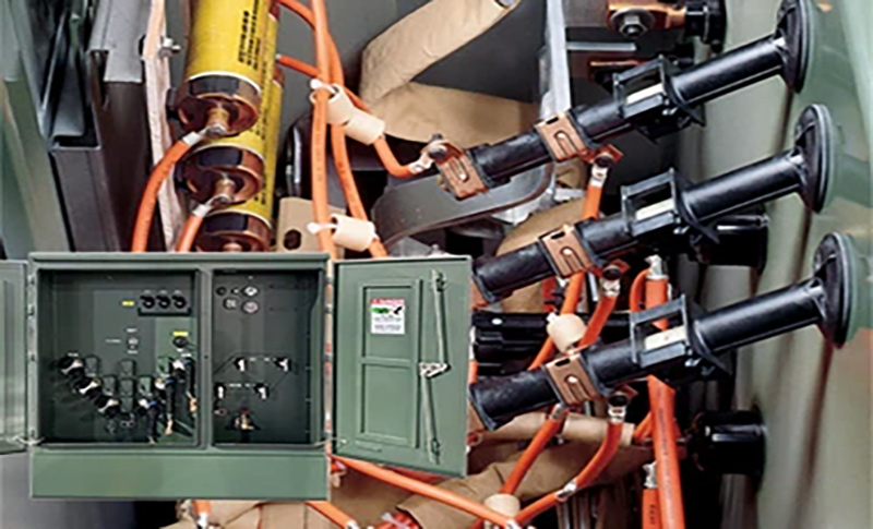
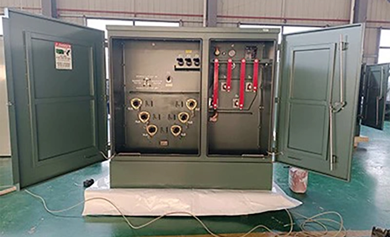
15 kV Bidirectional-Blocking SiC Device: Simplifying Medium-Voltage Topologies
Developed by Dr. Xing Huang during his tenure at the FREEDM Systems Center, North Carolina State University, the 15 kV SiC device addresses long-standing challenges in medium-voltage distribution networks. Currently, commercial SiC devices below 3 kV require multi-level cascaded H-bridge configurations to connect to 10–35 kV power grids, which leads to three critical issues:
- A large number of devices, increasing system footprint and material costs;
- Heightened control complexity, raising the threshold for system integration;
- Reduced system reliability, as more components increase the risk of failure.
The new 15 kV device—equipped with true bidirectional blocking capability and a 15 kV breakdown voltage—can directly interface with medium-voltage grids without multi-stage cascading, reducing the number of SST cascading levels by over 80%. A novel bidirectional terminal design, combined with extensive studies on short-circuit behavior, avalanche breakdown, and high-temperature aging, has enabled comprehensive reliability characterization, making the device suitable for demanding scenarios such as DC fault isolation and HVDC systems.
10 kV SiC MOSFET: Large Chip Area, High Current, and Mass-Production Readiness
At ISPSD 2025, Zhanxin Electronics and Zhejiang University unveiled a 10 kV SiC MOSFET that addresses two major industry pain points: large-area wafer fabrication and high-voltage conduction loss. Its key performance highlights are as follows:
- Chip size: 10 mm × 10 mm, one of the largest publicly reported for kV-class SiC MOSFETs;
- Conduction current: Approximately 40 A, meeting the high-power demands of medium-voltage applications;
- Breakdown voltage: Exceeding 12 kV, providing a safe margin for high-voltage operation;
- Specific on-resistance (Ron.sp): Below 120 mΩ·cm², approaching the theoretical limit of SiC materials;
- Manufactured on a 6-inch SiC platform, featuring scalable mass-production capability to support industrial application.
The device leverages high-energy ion implantation and a narrow JFET design to resolve the inherent trade-off between high voltage and low on-resistance. Meanwhile, optimized terminal structures have improved the yield of large-area chips, removing a key barrier to mass production.
Enabling Upgrades Across Smart Grids, AI Data Centers, and Renewable Energy
The maturation of kV-class SiC power devices is expected to accelerate the adoption of SSTs across multiple key sectors:
Smart Grids
SSTs integrated with medium-voltage SiC devices enable efficient AC–high-frequency–DC conversion, enhancing grid flexibility and facilitating the integration of distributed energy resources (e.g., rooftop PV, small wind power).
AI Data Centers
kV-class SiC devices make medium-voltage direct supply (MVDS) architectures feasible, bringing transformative benefits: single-rack power density can reach 1 MW, the power usage effectiveness (PUE) can drop below 1.1, and annual energy savings for hyperscale data centers can reach tens of millions of kilowatt-hours—significantly reducing operational costs and carbon emissions.
Renewable Energy
Thanks to the excellent high-frequency performance of kV-class SiC devices, PV inverters and wind converters can achieve remarkable improvements: filter size can be reduced by 50%, system cost can decrease by approximately 20%, and reliability is enhanced under harsh environmental conditions (e.g., high temperature, humidity, and voltage fluctuations).
Outlook: Higher Voltage, Lower Cost, and Wider Deployment
kV-class SiC devices are expected to evolve in three key directions:
- Higher performance: Pursuing higher breakdown voltages (15 kV+), higher current ratings, and lower energy loss through advanced technologies such as trench-gate structures and cutting-edge packaging;
- Cost reduction: Driving down costs via the adoption of 8-inch SiC wafers and continuous improvements in production yield;
- Deeper integration: Integrating more closely with SSTs to enable innovative topologies tailored for smart grids, AI computing clusters, and large-scale renewable energy bases.
These breakthroughs demonstrate strong momentum in China’s high-voltage SiC industrial ecosystem and signal a critical window of opportunity for the rapid industrialization of SSTs, which will play a pivotal role in advancing the global energy transition.